Nvidia over the years
The OG Tesla Architecture for GPGPU/ HPC:
https://www.cs.cmu.edu/afs/cs/academic/class/15869-f11/www/readings/lindholm08_tesla.pdf
Nvidia retired the Tesla brand in May 2020, reportedly because of potential confusion with the brand of cars.[1] Its new GPUs are branded Nvidia Data Center GPUs[2] as in the Ampere-based A100 GPU.[3]
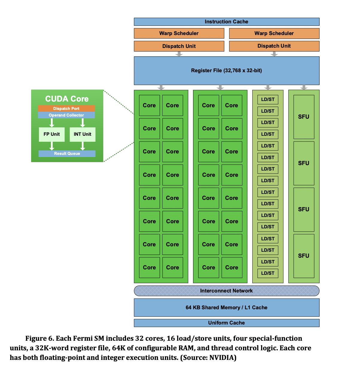
Nvidia FERMI
Nvidia “Fermi” External Contract Writeup
Fermi Whitepaper
NVIDIA Fermi contains
- 16 SMs
- 32 cores per SM, total 512 cores
- Each core contains a FP unti and INT unit
Interesting thing about Fermi: Each FP32 unit is capabable of also performing double precision operations in 2 clock cycles. This capability is not observed in later architectures, which always have dedicated FP64 units in them
Kepler Architecture - HPC and Consumer
https://en.wikipedia.org/wiki/Kepler_(microarchitecture)
https://www.nvidia.com/content/dam/en-zz/Solutions/Data-Center/tesla-product-literature/NVIDIA-Kepler-GK110-GK210-Architecture-Whitepaper.pdf
Had 192 FP32 and 64 FP64 units per SM
Maxwell Architecture - HPC and Consumer
https://en.wikipedia.org/wiki/Maxwell_(microarchitecture)
Had 128 FP32 and 4 FP64 units per SM
NVIDIA Pascal GPUs - HPC and Consumer - powering Tesla P100 and GTX 1080
https://en.wikipedia.org/wiki/Pascal_(microarchitecture)
Comparision: https://developer.nvidia.com/blog/inside-pascal/
https://www.es.ele.tue.nl/~heco/courses/ECA/GPU-papers/GeForce_GTX_1080_Whitepaper_FINAL.pdf
Volta - HPC - Tesla V100 - first gen tensor cores - architecture pdf
Compute Capability 7.0 (64 FP32, 64 INT32, 32 FP64 units) link
Turing - Consumer - RTX 20 series - 2nd gen tensor cores , 1st gen Ray tracing cores - architecture pdf -
Compute Capability 7.5 (note there are only 2 FP64 cores)
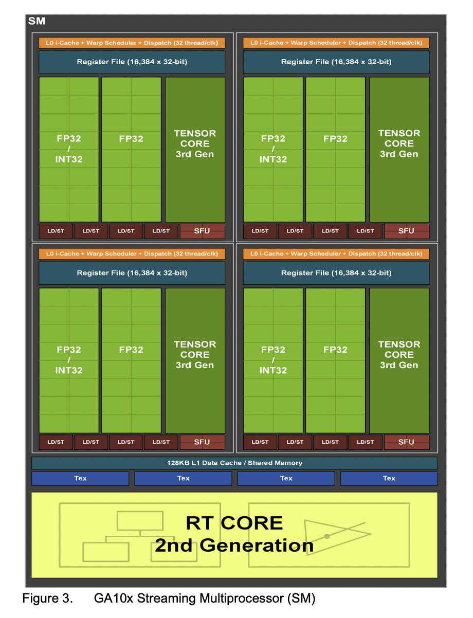
RTX 30 series GPUs, powered by Ampere GA10x architecture (slightly different than GA100 used for A100)
Each SM in GA10x GPUs contain:
- 128 FP32 CUDA Cores
- 2 FP64 CUDA Cores
- 64 INT32 CUDA Cores
- 4 third-generation Tensor Cores,
- Four Texture Units,
- one second-generation Ray Tracing Core, and 128 KB of L1/Shared Memory
All RTX 30 series GPUs have CUDA Compute Capability 8.6 link
Number of SMs vary in each GPU implementation of GA10x architecture
RTX 3060Ti has 38 SMs
RTX 3090 has 82 SMs
RTX 3090Ti has 84 SMs
About FP64 Support: The GA102 GPU (RTX 3090Ti) features 168 FP64 units (two per SM), which are not depicted in this diagram. The FP64 TFLOP rate is 1/64th the TFLOP rate of FP32 operations. The small number of FP64 hardware units are included to ensure any programs with FP64 code operate correctly, including FP64 Tensor Core code
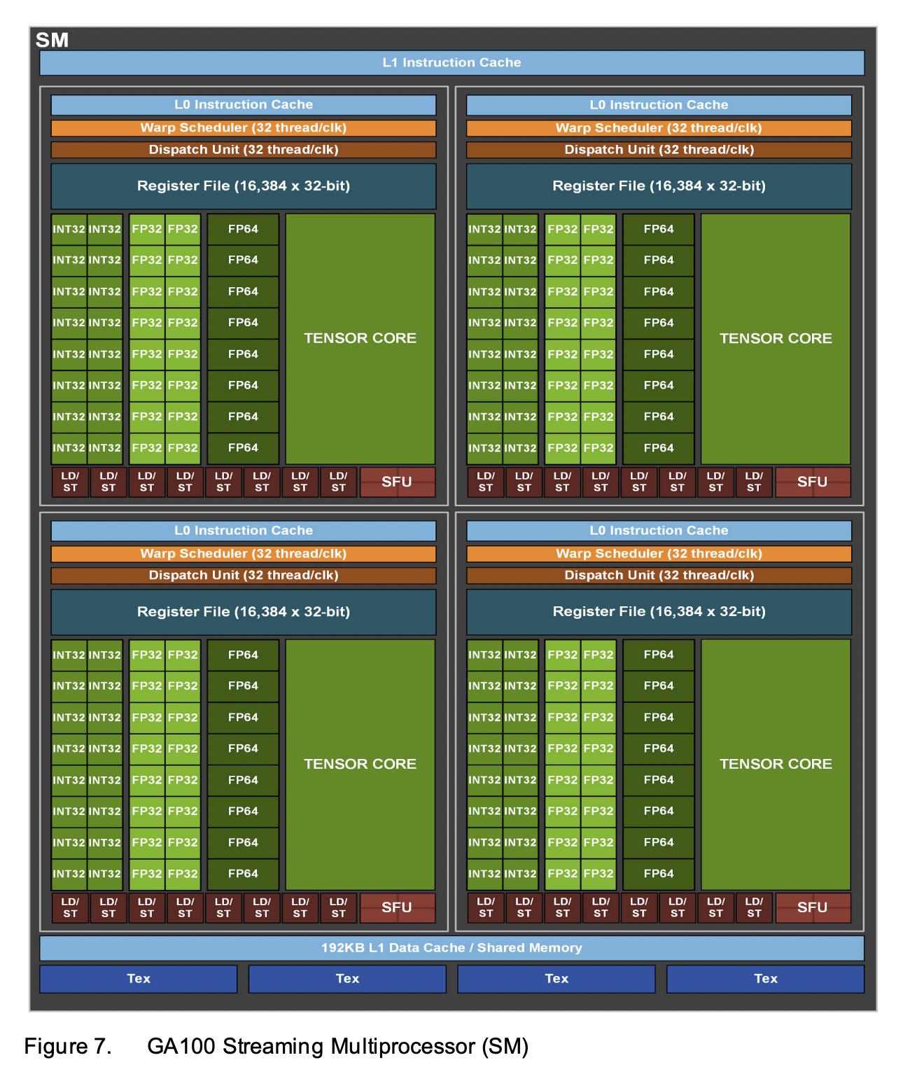
Nvidia A100 GPU powered by NVIDIA Ampere GA100 Architecture
Each SM in GA100 architecture contains:
- 64 FP32 and INT32 CUDA Cores
- 32 FP64 CUDA Cores,
- 4 Third-generation Tensor Cores
Nvidia A100 support CUDA Compute Capability 8.0 link
Number of SM may vary per implementation
The NVIDIA A100 Tensor Core GPU implementation of the GA100 GPU includes:
- 7 GPCs, 7 or 8 TPCs per GPC, 2 SMs per TPC, up to 16 SMs/GPC, 108 SMs
- 5 HBM2 stacks, 10 512-bit Memory Controllers
SM in NVIDIA GA100 Ampere Architecture (used in A100 series)
Hopper Microarchitecture - HPC - H100
https://en.wikipedia.org/wiki/Hopper_(microarchitecture)
Whitepaper: https://resources.nvidia.com/en-us-tensor-core/gtc22-whitepaper-hopper
Datasheet:
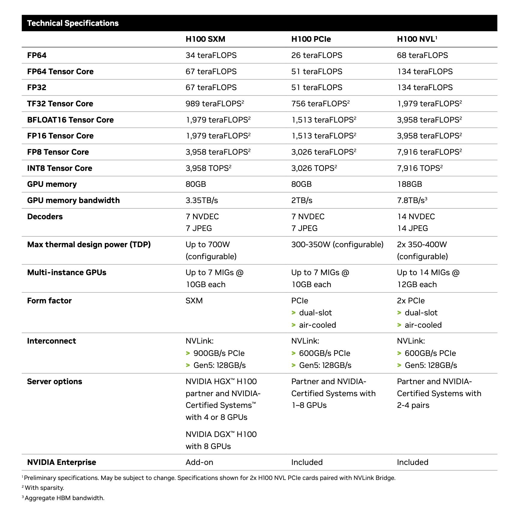
NVIDIA H100 GPU contains total 132 SMs per GPU
Each SM has (compute capability 9.0 for H100)
- 128 FP32 cores for single-precision arithmetic operations,
- 64 FP64 cores for double-precision arithmetic operations,
- 64 INT32 cores for integer math,
- 4 mixed-precision fourth-generation Tensor Cores supporting the new
FP8input type in eitherE4M3orE5M2for exponent (E) and mantissa (M), half-precision (fp16),__nv_bfloat16,tf32, INT8 and double precision (fp64) matrix arithmetic (see Warp Matrix Functions for details) with sparsity support, - 16 special function units for single-precision floating-point transcendental functions
- 4 texture units
- 4 warp schedulers
Ada Lovelace - Consumer - RTX 40 series
https://en.wikipedia.org/wiki/Ada_Lovelace_(microarchitecture)
Whitepaper: https://images.nvidia.com/aem-dam/Solutions/Data-Center/l4/nvidia-ada-gpu-architecture-whitepaper-v2.1.pdf
RTX 4090 GPU (AD102 architecture) contains total 144 SMs
Each SM contains (compute capability 8.9 for RTX 4090)
- 128 FP32 CUDA Cores
- 2 FP64 CUDA Cores
- 64 INT32 CUDA Cores
- 16 special function units
- 4 fourth-generation Tensor Cores
- 4 texture units
- one third-generation Ray Tracing Core
- 4 warp schedulers.
References
- Cuda Architecture capability:
Gives info on number of functional units per SM
https://docs.nvidia.com/cuda/cuda-c-programming-guide/index.html#architecture-8-x
GPUs with their Cuda compatibility:
https://developer.nvidia.com/cuda-gpus - All HPC/GPGPU offerings: https://en.wikipedia.org/wiki/Nvidia_Tesla